Skip to content

Define how specular_weight interacts with thin-film iridescence - #320

Open
jamportz wants to merge 5 commits into
AcademySoftwareFoundation:dev_1.2from
jamportz:thin_film_specular_weight
Open

jamportz wants to merge 5 commits into
AcademySoftwareFoundation:dev_1.2from
jamportz:thin_film_specular_weight

Conversation

@jamportz

@jamportz jamportz commented Sep 29, 2026 •

Copy link
Copy Markdown
Contributor

Fixes #319.

Summary

The spec did not say how specular_weight interacts with thin-film iridescence, and the reference graph used different rules for metal and dielectric bases (see #319). This PR specifies that specular_weight modulates the base beneath the film, rather than scaling the film's reflection, in the same way as it modulates the base without a film:

  • Dielectric base: the film sits on a substrate with the modulated IOR $\eta'$ (equation modulated_ior). The graph already did this.
  • Metallic base: $\xi_s$ multiplies the metal's Fresnel factor. No physical substrate does that, since a physical Fresnel factor always tends to 1 at grazing. So $w = \min(\xi_s, 1)$ is read as the fractional coverage of the metal beneath the film, with the rest index-matched to the surrounding medium. The film covers both:
$$\mathbf{R}_\mathrm{film}(\mu) = w\, \mathbf{R}_\mathrm{film}(\mu;\, \tilde{\mathbf{n}}) + (1 - w)\, \mathbf{R}_\mathrm{film}(\mu;\, 1)$$

Here $\tilde{\mathbf{n}}$ is the effective complex IOR of the (unscaled) metal, and $\mathbf{R}_\mathrm{film}(\mu;\, 1)$ is a free-standing film. With $T$ = thin_film_weight, the Fresnel factor of the film-covered base is $(1 - T)\, \mathbf{F}_\textrm{no film}(\mu) + T\, \mathbf{R}_\mathrm{film}(\mu)$.

Properties:

  • A vanishingly thin film has no effect, for any specular_weight and both base types.
  • As specular_weight → 0, both base types leave a free-standing film, still controlled by thin_film_weight.
  • With no film, or with specular_weight ≥ 1, nothing changes.
  • Fully consistent with #316 (the clamping of the metallic specular_weight boost), which is now in dev_1.2 and merged into this branch. See Consistency with #316 below.

This replaces the first version of this PR ("option B"), which evaluated the metal film on a conductor whose colors were scaled by $w$. As @sherholz pointed out, that made a zero-thickness film look different from no film whenever specular_weight < 1. The details are in this comment on #319.

Changes

Spec (index.html)

  • Metallic Base: a sentence stating that $\min(\xi_s, 1)$ acts as the fractional coverage of the metal beneath a film.
  • Thin-film iridescence: a new bullet stating the rule, followed by a paragraph defining the film reflectance for each base type (new equation thin_film_metal), and the blend equation thin_film_fresnel.

Reference MaterialX graph (reference/open_pbr_surface.mtlx)

  • Dielectric: unchanged. The film branch already receives the modulated IOR modulated_eta_s.
  • Metal: in each film lobe (main and haze), a reflection-only dielectric_bsdf with ior = 1 carrying the film (i.e. a free-standing film) is added to the existing film-covered generalized_schlick_bsdf. Its weight is 1 - metal_weight, where metal_weight = min(specular_weight, 1) is the overall metal weight from #316. The new nodes are metal_film_uncovered, metal_bsdf_tf_free_film and metal_bsdf_tf_covered, plus the haze equivalents.

Consistency with #316

This PR is fully consistent with #316, which is now in dev_1.2; I have merged dev_1.2 into this branch.

  • Same weight. #316 writes the metal Fresnel factor as $\min(\xi_s, 1)\, \mathbf{F}_{82}(\mu)$ (equation metal_fresnel), with the colors $\mathbf{F}_0$ and $\mathbf{C}_s$ boosted by $\max(\xi_s, 1)$ and clamped (equation metal_colors). The coverage $w = \min(\xi_s, 1)$ here is exactly that overall weight. In the graph, the free-standing film is weighted by 1 - metal_weight, using #316's own node.
  • Same colors. The film-covered metal uses the same (boosted) colors as the film-free metal.
  • $\xi_s \le 1$: the colors are not boosted, and this PR behaves exactly as before the merge. Re-rendering the metal after the merge (at $\xi_s$ = 0.5 and 0) gives results pixel-identical to the renders below.
  • $\xi_s &gt; 1$: $w = 1$, so there is no free-standing film term, and the film simply sits on the boosted metal. This PR does not change the boost or the clamp.
  • A vanishingly thin film has no effect for any $\xi_s$. In the merged graph, a zero-thickness film renders pixel-identically to no film at $\xi_s$ = 0.5 and at 1.5 (MaterialXView).

Renders

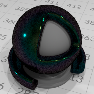
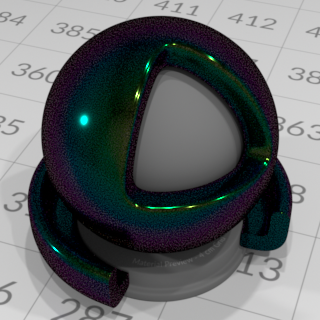
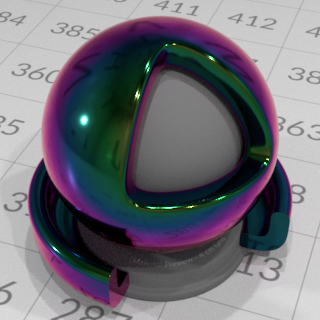
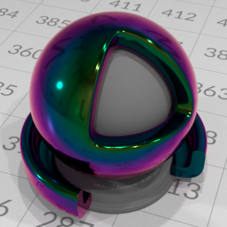
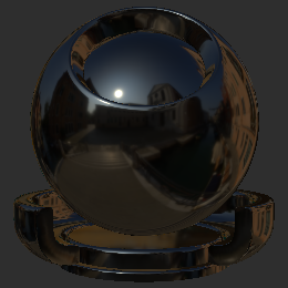
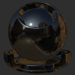
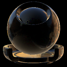
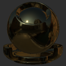
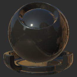
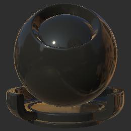
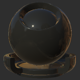
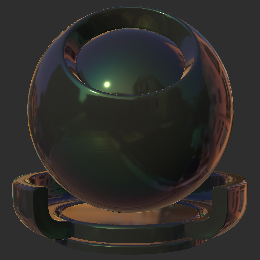
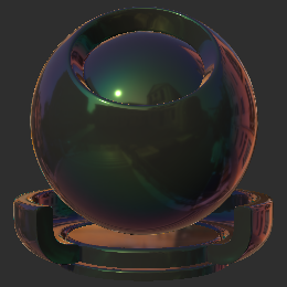
The metal (base_color 0.91) and a near-black dielectric, each with a 0.5 µm film of IOR 1.4, specular_roughness 0.1 and thin_film_weight = 1. Rendered in Arnold 7.5.4, from the graphs compiled to OSL.

$\xi_s$ 1 0.5 0.01 0
Metal
dev_1.2
Metal
this PR
Dielectric
dev_1.2 and this PR
  • At $\xi_s = 1$, the metal is pixel-identical to dev_1.2.
  • At $\xi_s = 0$, the metal gives the same free-standing film as the dielectric. In dev_1.2 the film vanished on the metal.
  • The dielectric renders are pixel-identical before and after.

Zero-thickness film (thin_film_thickness = 0, thin_film_weight = 1). This should look exactly like no film. It is rendered in MaterialXView, because Arnold's OSL conductor_bsdf (used by option B) doesn't honor ior/extinction.

no film option B (first version) this PR option B − no film (×4) this PR − no film (×4)
$\xi_s = 0.5$
$\xi_s = 0.1$

Notes

  • Implementations must not skip the specular lobe when $\xi_s = 0$ if thin_film_weight > 0, since the film is still present.
  • Native implementations need no extra closure. The coverage blend sits inside a single Fresnel factor: two film evaluations sharing the microfacet distribution.
  • Validation. With #317 now in dev_1.2, the graph validates cleanly.
  • MaterialX GLSL thin film on generalized_schlick_bsdf. In MaterialXView, a film-covered generalized_schlick_bsdf renders about 40% too dark. In mx_fresnel_airy, the Schlick branch sets R23p = R23s = 0.5 * f where each should be f. This affects dev_1.2 equally and is a separate MaterialX issue. Arnold's own closure is unaffected, which is why the main renders above use Arnold.

🤖 Generated with Claude Code

jamportz and others added 2 commits September 29, 2026 17:36
…cademySoftwareFoundation#319)

Clarify in the spec that specular_weight acts on the base beneath a thin
film rather than scaling the film's reflection: the film is evaluated on a
substrate whose reflectivity is modulated by specular_weight (the modulated
IOR for dielectrics; the complex IOR of the w-scaled metal colors for
metals, w = min(specular_weight, 1)), blended with the film-free Fresnel
by thin_film_weight. As specular_weight -> 0 a free-standing film remains.

In the reference graph the dielectric branch already behaves this way. The
metal thin-film branch now evaluates the film on a conductor_bsdf whose
ior/extinction come from artistic_ior of the w-scaled colors, instead of
weighting the film-covered generalized_schlick_bsdf by specular_weight.

Co-Authored-By: Claude Opus 5.5 (1M context) <noreply@anthropic.com>
@jamportz jamportz changed the title Thin film: specular_weight modulates the substrate beneath the film Define how specular_weight interacts with thin-film iridescence Sep 29, 2026
@jamportz

jamportz commented Oct 13, 2026 •

Copy link
Copy Markdown
Contributor Author

Update: this PR has now been revised to option C (description updated). It is fully consistent with #316; see the description.

Following @sherholz's review in #319, the first version of this PR (option B) failed a basic requirement for metals: a film of vanishing thickness should look exactly like no film. When $\xi_s$ < 1, the film-free lobe ($w\,\mathbf{F}_{82}$, which tends to $w$ at grazing) and the film lobe (a conductor with the scaled colors, which tends to 1 at grazing) are different BSDFs, even at zero thickness. So thin_film_weight changes the look even when there is no film. The details and renders are in this comment on #319.

I've revised the metal part of this PR to "option C". Here $\xi_s$ on a metal acts as the coverage $w = \min(\xi_s, 1)$ of the metal beneath the film, and the film covers both the metal and the uncovered remainder:

$$\mathbf{F}_\mathrm{metal}(\mu) = (1 - T)\, w\, \mathbf{F}_{82}(\mu) \;+\; T \Bigl[\, w\, \mathbf{R}_\mathrm{film}(\mu;\, \tilde{\mathbf{n}}) \;+\; (1 - w)\, \mathbf{R}_\mathrm{film}(\mu;\, 1) \,\Bigr]$$

$\tilde{\mathbf{n}}$ is the effective complex IOR of the unscaled metal, and $\mathbf{R}_\mathrm{film}(\mu;\, 1)$ is a free-standing film. With this rule:

  • A zero-thickness film looks exactly like no film, for every $\xi_s$.
  • The film still remains at $\xi_s = 0$, matching the dielectric base.
  • Nothing changes at $\xi_s = 1$ or without a film.

Changes

Graph (prototyped on dev_1.2; diff below)

  • Revert the metal film lobes (metal_bsdf_tf, metal_bsdf_haze_tf) to the dev_1.2 film-covered generalized_schlick_bsdf, weighted by specular_weight. This drops the artistic_ior and conductor_bsdf nodes. That also sidesteps the Arnold OSL conductor_bsdf problem, and the fact that artistic_ior's edge_color is Gulbrandsen's edge tint rather than the reflectance at 82°.
  • Add a reflection-only dielectric_bsdf with ior = 1 carrying the film, weighted by 1 - min(specular_weight, 1). add it to each metal film lobe.
  • Dielectric: unchanged.

Spec

  • Metallic base: the film reflectance becomes $w\,\mathbf{R}_\mathrm{film}(\mu;\, \tilde{\mathbf{n}}) + (1 - w)\,\mathbf{R}_\mathrm{film}(\mu;\, 1)$, instead of a film on a substrate with scaled colors.
  • Dielectric base: unchanged ($\mathbf{R}_\mathrm{film}$ on the modulated IOR $\eta'$).
  • Common to both: as $\xi_s \to 0$ both reduce to a free-standing film, still controlled by thin_film_weight. The blend $(1 - T)\,\mathbf{F}_\textrm{no film} + T\,\mathbf{R}_\mathrm{film}$ (equation thin_film_fresnel) stays as written.
Graph diff (against dev_1.2)
<!-- after metal_bsdf_tf -->
<min name="metal_film_coverage" type="float">
  <input name="in1" type="float" nodename="specular_weight_nonnegative" />
  <input name="in2" type="float" value="1.0" />
</min>
<subtract name="metal_film_uncovered" type="float">
  <input name="in1" type="float" value="1.0" />
  <input name="in2" type="float" nodename="metal_film_coverage" />
</subtract>
<dielectric_bsdf name="metal_bsdf_tf_free_film" type="BSDF">
  <input name="weight" type="float" nodename="metal_film_uncovered" />
  <input name="ior" type="float" value="1.0" />
  <input name="roughness" type="vector2" nodename="main_roughness" />
  <input name="normal" type="vector3" interfacename="geometry_normal" />
  <input name="tangent" type="vector3" interfacename="geometry_tangent" />
  <input name="scatter_mode" type="string" value="R" />
  <input name="thinfilm_thickness" type="float" nodename="thin_film_thickness_nm" />
  <input name="thinfilm_ior" type="float" nodename="thin_film_ior_nonnegative" />
</dielectric_bsdf>
<add name="metal_bsdf_tf_covered" type="BSDF">
  <input name="in1" type="BSDF" nodename="metal_bsdf_tf" />
  <input name="in2" type="BSDF" nodename="metal_bsdf_tf_free_film" />
</add>
<!-- metal_bsdf_tf_mix: fg = metal_bsdf_tf_covered (was metal_bsdf_tf) -->

<!-- same for the haze lobe, with haze_roughness: metal_bsdf_haze_tf_free_film, metal_bsdf_haze_tf_covered -->

Renders

The metal (base_color 0.91, 0.5 µm film of IOR 1.4, specular_roughness 0.1, thin_film_weight = 1) in Arnold 7.5.4. Option C is the graph above compiled to OSL. Option B is the Arnold prototype from #319.

$\xi_s$ 1 0.5 0.01 0
dev_1.2 graph
option B (first version)
option C (this PR)

Zero-thickness film (thin_film_thickness = 0, thin_film_weight = 1), rendered in MaterialXView. This should look exactly like no film:

no film option B option C option B − no film (×4) option C − no film (×4)
$\xi_s = 0.5$
$\xi_s = 0.1$

Correction to the PR description

The first version of the description attributed the look change at $\xi_s = 1$ ("less yellow at the rim") to evaluating the film on a genuine conductor. In fact, much of the before/after difference in those MaterialXView renders comes from a MaterialX GLSL bug.

In mx_fresnel_airy, the Schlick branch (used by generalized_schlick_bsdf) sets R23p = R23s = 0.5 * f, where each should be f. The other branches use the full per-polarization reflectances. As a result, a film-covered generalized_schlick_bsdf renders about 40% too dark in MaterialXView, even at vanishing film thickness. For base_color 0.91, a 1 nm film gives 0.57 at normal incidence instead of about 0.91.

Arnold's own implementation of the closure doesn't show this. The bug is still present on MaterialX main and should be reported there separately. With option C, the metal film at $\xi_s = 1$ is unchanged from dev_1.2.

jamportz and others added 2 commits October 13, 2026 13:41
…he film (AcademySoftwareFoundation#319)

Replace the scaled-color conductor substrate with a coverage interpretation:
the film covers a fraction w = min(specular_weight, 1) of metal and a fraction
1 - w index-matched to the surrounding medium (a free-standing film). A
vanishingly thin film then has no effect for any specular_weight, while the
film still remains at specular_weight = 0. Nothing changes at
specular_weight >= 1 or without a film.

Graph: the metal film lobes revert to the dev_1.2 film-covered
generalized_schlick_bsdf, and a reflection-only dielectric_bsdf (ior 1, with
the film), weighted by 1 - min(specular_weight, 1), is added to each.

Co-Authored-By: Claude Opus 5.5 <noreply@anthropic.com>
@jamportz
jamportz marked this pull request as ready for review October 27, 2026 13:49
…on#317) into thin_film_specular_weight

Resolve conflicts with AcademySoftwareFoundation#316: keep its metal Fresnel text and refer the thin-film
coverage sentence to equation metal_fresnel; the film-covered metal now uses the
colors of equation metal_colors. In the graph, use AcademySoftwareFoundation#316's metal_weight as the
film coverage instead of a duplicate min(specular_weight, 1) node.

Co-Authored-By: Claude Opus 5.5 <noreply@anthropic.com>
jamportz added a commit to jamportz/OpenPBR that referenced this pull request Nov 3, 2026
…dation#320

Co-Authored-By: Claude Opus 5.5 <noreply@anthropic.com>
@jamportz

jamportz commented Nov 3, 2026 •

Copy link
Copy Markdown
Contributor Author

Option D (for discussion): specular_weight modulates the metal's complex IOR, as it already does the dielectric's IOR

This is a separate proposal, not what this PR currently implements (option C). It is posted here so that the two can be compared.

The idea

For a dielectric base, specular_weight already works by lowering the IOR, so that the reflectance at normal incidence is multiplied by $\xi_s$ (equation modulated_ior). Option D applies the same operation to a metal, using its complex IOR. Both base types then follow a single rule:

specular_weight scales the base's reflectance at normal incidence by modulating its (real or complex) IOR.

Thin film then needs no special treatment. For both base types, the film sits on the modulated substrate.

The math

Dielectric (current spec, rewritten). Let $r_0 = (\eta - 1)/(\eta + 1)$ be the reflection amplitude at normal incidence, so that $F_0 = r_0^2$. Equation modulated_ior is then exactly

$$r_0' = \sqrt{\xi_s}\; r_0 \ , \qquad \eta' = \frac{1 + r_0'}{1 - r_0'}$$

since its $\epsilon = \mathrm{sgn}(\eta - 1)\sqrt{\xi_s F_0}$ is $\sqrt{\xi_s}\, r_0$. The reflectance at normal incidence becomes $\xi_s F_0$, and the sign (phase) of $r_0$ is unchanged.

Metal (option D).

  1. The metal's complex IOR. Let $\tilde{n} = n + i k$ (at each wavelength, or per channel in an RGB renderer) be the IOR of the conductor whose Fresnel factor reproduces the metal's reflectance $\mathbf{F}_0$ at normal incidence and $\mathbf{F}(\bar\mu) = \mathbf{C}_s\, \mathbf{F}_\mathrm{Schlick}(\bar\mu)$ at 82°. This $\tilde{n}$ is unique. Among complex IORs with a given $F_0$, the reflectance at 82° varies monotonically. So $\tilde{n}$ is fixed by the metal's two colors alone, and the spec doesn't need to prescribe a particular mapping. (For example, Gulbrandsen's mapping gives this $\tilde{n}$ if its edge tint is solved for so as to match $F(\bar\mu)$. I also have an exact and cheap inversion, a closed form plus a few Newton steps, from a paper in preparation.)
  2. The same modulation as the dielectric, with the complex amplitude, where $w = \min(\xi_s, 1)$:
$$\tilde{r}_0 = \frac{\tilde{n} - 1}{\tilde{n} + 1} \ , \qquad \tilde{r}_0' = \sqrt{w}\; \tilde{r}_0 \ , \qquad \tilde{n}' = \frac{1 + \tilde{r}_0'}{1 - \tilde{r}_0'}$$

This multiplies the reflectance at normal incidence by exactly $w$ and keeps the phase of $\tilde{r}_0$. For a metal, that phase is what distinguishes free-electron from interband behavior. For $k = 0$ it reduces to equation modulated_ior.

  1. Fresnel factors. $\mathbf{F}_\mathrm{metal}(\mu) = F_\mathrm{conductor}(\mu;\, \tilde{n}')$, and with a film $\mathbf{R}_\mathrm{film}(\mu;\, \tilde{n}')$, blended by thin_film_weight as usual. For $\xi_s &gt; 1$, $w = 1$, and $\tilde{n}$ comes from the boosted colors of #316.

Why keep the phase, rather than scale both colors and invert again? The scaled pair $(w F_0,\, w F(\bar\mu))$ soon becomes unreachable by any physical material. For $F_0 = 0.91$ with a white edge, at $w = 0.25$ the scaled 82° target is 0.238, but the lowest 82° reflectance of any material with normal reflectance 0.228 is 0.489. Keeping the phase fixed always gives a valid IOR, varies smoothly with $\xi_s$, and reaches $\tilde{n}' = 1$ at $\xi_s = 0$.

Properties

  • One rule for both bases. The reflectance at normal incidence is exactly $\xi_s F_0$, and the curve away from normal incidence is that of a physical (real or complex) IOR. So this is more consistent with the "physically-based" dielectric behaviour than the other proposals.
  • At $\xi_s = 0$, $\tilde{n}' = 1$, so the metal vanishes. With a film, a free-standing film remains, as for the dielectric (and as in option C).
  • A zero-thickness film looks exactly like no film, since both lobes use the same $\tilde{n}'$. Verified pixel-identical at $\xi_s$ = 0.5 and 0.1.
  • $\xi_s &gt; 1$: unchanged from #316.

How it differs from option C

The two options agree at $\xi_s = 0$ and (nearly) at $\xi_s = 1$. In between:

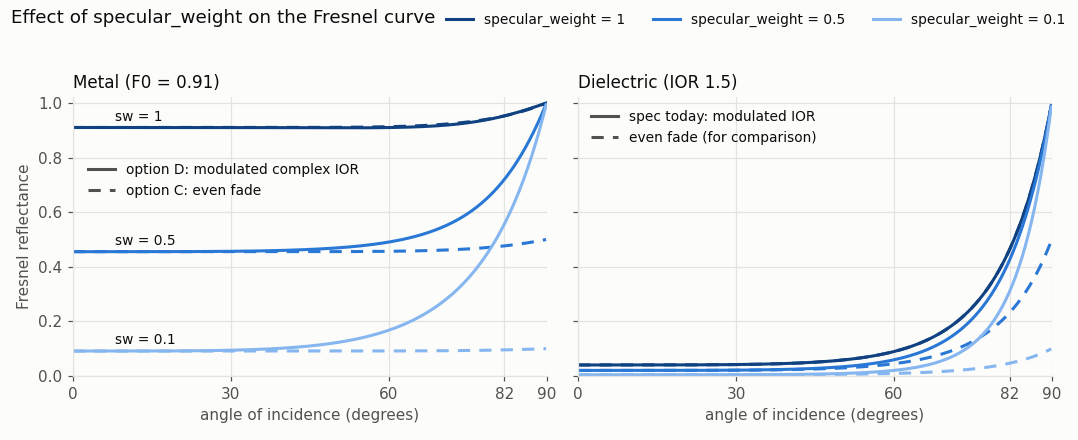
  • A metal no longer fades evenly as $\xi_s$ decreases. As with the dielectric today, the rim stays bright. For the grey metal below, the reflectance at 82° is:

    • $\xi_s = 0.5$: 0.72 under option D, against 0.48 under option C;
    • $\xi_s = 0.1$: 0.56 against 0.095.

    For comparison, the IOR 1.5 dielectric at $\xi_s = 0.1$ gives 0.31 under the current spec, against 0.046 for an even fade. This changes the look of every metal with $\xi_s &lt; 1$, with or without a film, compared with 1.0–1.2.

  • At $\xi_s = 1$, the metal becomes the conductor $\tilde{n}$ rather than the F82-tint curve. The two agree exactly at 0° and 82° and differ slightly elsewhere: 0.2% in mean brightness for the grey metal below. To keep F82-tint exactly at $\xi_s = 1$, one could use $\mathbf{F}_{82}(\mu)\, F_\mathrm{conductor}(\mu;\, \tilde{n}') / F_\mathrm{conductor}(\mu;\, \tilde{n})$ instead.

  • With a film, the fringes are most vivid at intermediate $\xi_s$, because the substrate's reflection is brought down towards the film's own.

  • Implementation.

    • Renderers: each needs the $(\mathbf{F}_0, \mathbf{F}(\bar\mu)) \to \tilde{n}$ inversion and a complex Fresnel factor for the metal.
    • MaterialX graph: there is no node for the inversion (artistic_ior takes Gulbrandsen's edge tint, which is not the 82° reflectance), so it would have to be built from math nodes or added as a new node.
    • Arnold: its OSL conductor_bsdf currently ignores ior/extinction.

RGB and spectral rendering

The inversion and modulation are defined at each wavelength, in the same way as the spec's treatment of dispersion. The colors $\mathbf{F}_0$ and $\mathbf{F}(\bar\mu)$ are turned into reflectance spectra, and $\tilde{n}(\lambda)$ is found and modulated at each wavelength (the factor $\sqrt{w}$ is the same at every wavelength).

  • At normal incidence, the result is exactly $w\,\mathbf{F}_0$ in any renderer, because the scaling is linear.
  • Away from normal incidence, the modulated reflectance is a nonlinear function of the colors. So evaluating it separately per RGB channel, as in the renders below, is only an approximation of the spectral result. The same is true of thin film on a metal under either option. Per-channel optical constants under a film can be visibly off.

An RGB renderer can avoid this with the "locally spectral" approach that the Adobe Standard Material uses for dispersion (Kutz, Hašan and Edmondson, Novel aspects of the Adobe Standard Material, 2021, section 4):

  1. Each color channel samples a wavelength from its own distribution (sensor sensitivity times illuminant).
  2. The metal's Fresnel factor, including any film, is evaluated at that wavelength.
  3. The result is accumulated in that channel.

With the colors converted to spectra consistently with those distributions, this gives the spectrally integrated color in expectation, at the cost of some color noise. Option D, and thin film on a metal, then behave the same in RGB and spectral renderers.

Renders

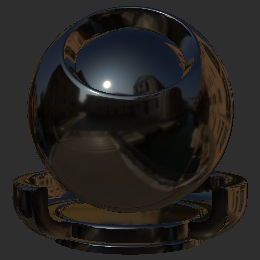
These were rendered in MaterialXView (GLSL), with specular_roughness 0.1 and the film at 0.5 µm and IOR 1.4.

  • Option D: $\tilde{n}'$ was computed per material with the inversion and modulation above, and passed to conductor_bsdf. This is a prototype, not a full graph implementation.
  • Option C: the film-covered metal lobe was likewise evaluated on conductor_bsdf, with the unmodulated $\tilde{n}$.

So both options use the same film code, which also avoids the GLSL thin-film bug in generalized_schlick_bsdf.

Bare base (no film)

specular_weight 1 0.5 0.25 0.1 0
Grey metal
option C
Grey metal
option D
Gold
option C
Gold
option D
Dielectric
(current spec)

With film

specular_weight 1 0.5 0.25 0.1 0
Grey metal
option C
Grey metal
option D
Dielectric
(current spec)

The grey metal has base_color 0.91 and a white specular_color. The gold is the repository's open_pbr_gold colors. The dielectric has a near-black base and specular_ior 1.5, and it is the same under both options.

Summary

Option C (this PR) Option D
Rule Metal: coverage of the metal beneath the film Both bases: modulate the (complex) IOR
Metal without film, $\xi_s &lt; 1$ Unchanged (even fade) Rim stays bright, like the dielectric
Metal at $\xi_s = 1$ Unchanged Conductor $\tilde{n}$ (matches F82-tint at 0° and 82°)
$\xi_s = 0$ Metal vanishes; with film, free-standing film Same
Zero-thickness film = no film Yes Yes
$\xi_s &gt; 1$ (#316) Unchanged Unchanged
Scope Clarifies film behavior only Changes the metal model

Option D is the more consistent model, but it changes existing metals. Option C is the minimal change for 1.2. Opinions welcome.

@sherholz

sherholz commented Nov 3, 2026

Copy link
Copy Markdown

@jamportz sounds like an interesting alternative. Could you add a column of weights closer to 0.0: like 0.025, 0.01, just to see if it fades out or makes a sudden disappearance.

For the Fresnel plots it would be interesting to start with a F0 and F82 setup and also plot a version with wF0 and wF82 compared to the new proposal. That should strengthen the Why keep the phase, rather than scale both colors and invert again? section.

jamportz added a commit to jamportz/OpenPBR that referenced this pull request Nov 3, 2026
…on#320

Co-Authored-By: Claude Opus 5.5 <noreply@anthropic.com>
@jamportz

jamportz commented Nov 3, 2026

Copy link
Copy Markdown
Contributor Author

Here is GLSL for the $(\mathbf{F}_0, \mathbf{F}(\bar\mu)) \to \tilde{n}$ inversion that option D needs, per color channel (or per wavelength). It is the closed form from the paper in preparation, which is exact in the good-conductor (surface-impedance) limit. It reproduces $F_0$ exactly, and the rest of the Fresnel curve to within about 0.01 for real metals. A few Newton steps along the family of conductors with the same $F_0$ make it exact. I've left those out here.

The second function is the option D modulation of $\tilde{n}$ by specular_weight.

// Complex IOR (n, k) of the conductor whose reflectance is F0 at normal incidence and F82 at 82 degrees,
// at one wavelength or color channel. In OpenPBR terms, per channel:
//     F0  = base_color
//     F82 = specular_color * (F0 + (1 - F0) * pow(1 - cos(82 degrees), 5))
// Closed form in the good-conductor (surface-impedance) limit. It reproduces F0 exactly, and the rest of
// the Fresnel curve approximately. A few Newton steps make it exact.
vec2 conductor_ior_from_F0_F82(float F0, float F82)
{
    const float mu = 0.1391731;                     // cos(82 degrees)
    F0 = clamp(F0, 0.0, 0.9999);
    float a = mu * (1.0 - F0) / (1.0 + F0);
    float u = 1.0 - F82;
    float b = 2.0*a*((1.0 + mu*mu)*F82 + a*(1.0 + F82));
    float h = (b - (1.0 + mu*mu*mu*mu)*u) / min(2.0*mu*mu*u - b, -1e-9);
    h = max(h, 1.0);

    // |z|^2, where z = 1/(n + ik) is the surface impedance: the root of |z|^2 + 1/|z|^2 = 2h with |z| <= 1.
    // It is clamped to the end of the range, the dielectric (k = 0) with this F0, which has the lowest F82.
    float r  = sqrt(F0);
    float z2 = max(1.0 / (h + sqrt(h*h - 1.0)), (1.0 - r)*(1.0 - r) / ((1.0 + r)*(1.0 + r)));
    float z  = sqrt(z2);
    float c  = min(a * (1.0 + z2) / (2.0*mu*z), 1.0);   // cosine of the phase of z
    return vec2(c, sqrt(1.0 - c*c)) / z;               // (n, k)
}

// Option D: specular_weight w in [0, 1] scales the normal-incidence amplitude r0 = (eta - 1)/(eta + 1) by sqrt(w),
// keeping its phase, as the spec's modulated IOR does for a dielectric.
vec2 cdiv(vec2 a, vec2 b) { return vec2(a.x*b.x + a.y*b.y, a.y*b.x - a.x*b.y) / dot(b, b); }

vec2 modulate_ior(vec2 eta, float w)
{
    vec2 one = vec2(1.0, 0.0);
    vec2 r = sqrt(w) * cdiv(eta - one, eta + one);
    return cdiv(one + r, one - r);
}

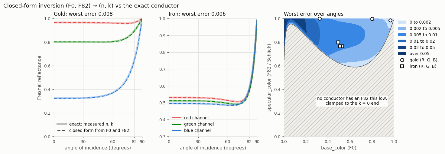
Closed-form inversion compared with the exact conductor

  • Real metals: for gold and iron (left, from typical RGB optical constants), the closed form (dashed) lies on the exact Fresnel curves. The worst errors over angles are 0.008 and 0.006.
  • All inputs: the right panel shows the worst error over angles across OpenPBR's (base_color, specular_color) square. Where a conductor exists, it is at most 0.011 for base_color ≥ 0.3 (median 0.005), which covers real metals. It only grows for dark metals with a high specular_color, where $|\tilde{n}|$ is small and the good-conductor limit no longer holds.
  • Inputs that no conductor matches: for a given $F_0$, the lowest 82° reflectance of any conductor is that of the dielectric ($k = 0$) at the end of the family, with $n = (1 + \sqrt{F_0})/(1 - \sqrt{F_0})$. Below the curve in the right panel (specular_color below about 0.6 for mid-range base_color, rising toward 1 for very dark or very bright ones), there is no matching $\tilde{n}$, so the code clamps to that end, which keeps $F_0$ exact. Real metals lie well above the curve, but option D would need to define $\tilde{n}$ there, and clamping is the natural choice.
  • Tested: the code compiles and runs on the GPU through MaterialX's GLSL renderer. It matches a float64 reference to $2 \times 10^{-6}$ in reflectance, with no NaNs or infinities for any $F_0$ and $F_{82}$ in $[0, 1]$ (checked in float32).

This branch has not been deployed

No deployments
Sign up for free to join this conversation on GitHub. Already have an account? Sign in to comment

Labels

None yet

Projects

None yet

Development

Successfully merging this pull request may close these issues.

2 participants